High-Density Interconnect (HDI) Printed Circuit Boards (PCBs) are revolutionizing electronic design, enabling higher performance in compact devices. With the increasing demand for miniaturization in consumer electronics, telecommunications, medical devices, and automotive applications, HDI PCB technology has become essential in modern manufacturing.Get more news about Hdi PCB,you can vist our website!
What is HDI PCB?
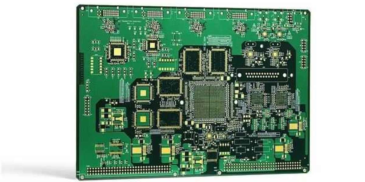
HDI PCB refers to printed circuit boards that use microvias, fine lines, and multilayer designs to achieve high-density connectivity in a smaller form factor. Compared to traditional PCBs, HDI PCBs feature improved electrical performance and enhanced reliability due to their advanced manufacturing techniques.
Some key characteristics of HDI PCBs include:
Microvias: Tiny holes used to create electrical connections between PCB layers.
Laser Drilling Technology: Enables precise formation of microvias.
Thin and Compact Layers: Reduces board thickness and weight while enhancing functionality.
High Signal Integrity: Minimizes electrical interference and improves high-speed performance.
Advantages of HDI PCB
The adoption of HDI PCB technology offers several benefits across industries:
Smaller Size, Increased Efficiency
HDI PCBs allow for more components to be placed in a smaller area, making them ideal for compact devices such as smartphones, laptops, and wearables.
Enhanced Electrical Performance
With shorter interconnection paths and reduced signal loss, HDI PCBs improve the speed and functionality of electronic devices.
Greater Reliability
HDI PCBs use advanced materials that enhance durability, making them suitable for medical and aerospace applications.
Cost-Effective Manufacturing
While HDI PCBs require specialized production processes, their ability to reduce component count and optimize circuit layouts can lower overall costs.
Applications of HDI PCB
HDI PCB technology is widely used in various industries, including:
Consumer Electronics: Smartphones, tablets, and smartwatches benefit from HDI PCBs due to their compact designs and high-performance capabilities.
Medical Devices: High-density interconnect technology is essential for precision equipment such as MRI scanners and implantable devices.
Automotive Electronics: Advanced driver assistance systems (ADAS) and electric vehicle components utilize HDI PCBs for improved efficiency.
Aerospace Defense: Satellites, radars, and military-grade communication systems depend on HDI PCBs for their reliability in extreme conditions.
Conclusion
HDI PCB technology is shaping the future of electronic devices by enabling miniaturization, enhancing reliability, and optimizing electrical performance. As industries continue to demand high-speed, compact, and efficient solutions, HDI PCBs will remain a cornerstone of advanced circuit design.